YSZ
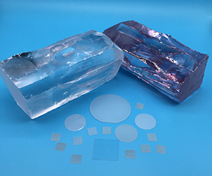
Zirconia(ZrO2) single crystal wafer is one of the most early high temperature superconducting substrate. Because Zirconia needs to be dopped with yttrium to stable its structure, normally the dopped yttrium dopped Zirconia(YSZ) single crystal is used. The mechanical stability and chemical stability of YSZ is excellent, and it has relatively lower price, which is especially applicable in making positive film.
使用/应用
Zirconia(ZrO2) single crystal wafer is one of the most early high temperature superconducting substrate. Because Zirconia needs to be dopped with yttrium to stable its structure, normally the dopped yttrium dopped Zirconia(YSZ) single crystal is used.
特点/优势
The mechanical stability and chemical stability of YSZ is excellent, and it has relatively lower price, which is especially applicable in making positive film.
-
Crystal Structure
Cubic
Growth Method
Electric-Arc fusion Method
Lattice Constant
a=5.147Å
Melting Point
2700℃
Density
6.0 (g/cm3)
Mhos Hardness
8-8.5 (mohs)
Purity
99.99%
Thermal Expansion
10.3×10⁻⁶/K
Dielectric Constant
ε=27
Dimension
10×3mm, 10×5mm, 10×10mm, 15×15mm, 20×15mm, 20×15mm
According to customer needs, substrates with special orientation and size can be customized.
Thickness
0.5mm,1.0mm
Dimensional Tolerance
<±0.1mm
Thickness Tolerance
<±0.015m, ±0.005mm for special needs)
Polishing
One side or two sides
Orientation
<100>、<110>、<111>etc.
Orientaion Tolerance
±0.5°
Edge Orientation Accuracy
2°(Special requirements can reach within 1°)
Chamfered Wafer
According to specific requirements, wafers with edge-oriented crystal planes inclined at a specific angle (inclination angle 1°-45°) can be processed.
Package
Class 100 clean bag, Class 1000 super clean room
-
Dimension
10×3mm, 10×5mm, 10×10mm, 15×15mm, 20×15mm, 20×15mm
Customize size and crystal orientation upon request.
Thickness
0.5mm,1.0mm
Dimensional Tolerance
<±0.1mm
Thickness tolerance
<±0.015m, ±0.005mm for special needs)